
basic FPGA stuff
To start up with FPGAs, the schematic approach is great, as it gives useable
results rather quick. I'll describe some solutions to basic problems here.
The choice of using the MaxPlus2 software from Altera is arbitrary, I assume
others are behaving similar and exhibit similar features.
The ever to be repeated mantra is : synchroneous is good, asynchroneous is bad
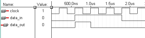
Synchronizing a signal to the clock
Generally done with a flipflop

As can be seen, the output changes state on the rising input. All external signals
should be synchronized to the clock before further use.
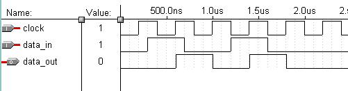
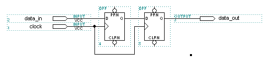
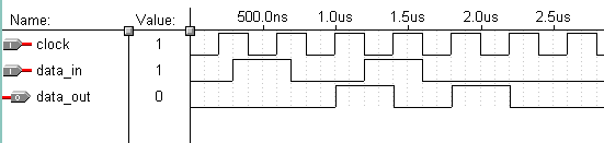
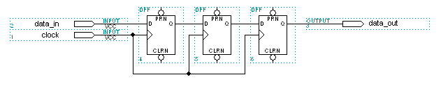
Delay of a signal
A signal is delayed by an integer number of clock cycles by flipflops
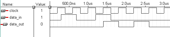
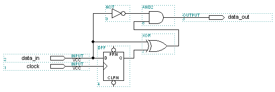
Detecting a signal change
Detecting a change in a signal is as simple as a flipflop plus an XOR.
Here a pulse is created upon a signal change.
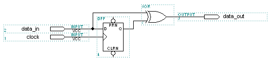
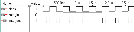
If only the rising slope is of interest, mask the other
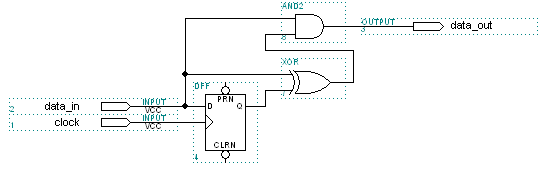
If only the falling slope is of interest, mask the other

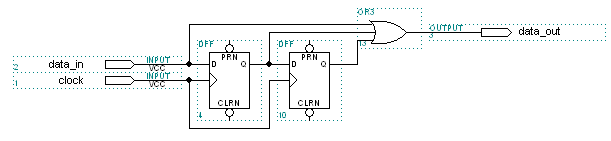
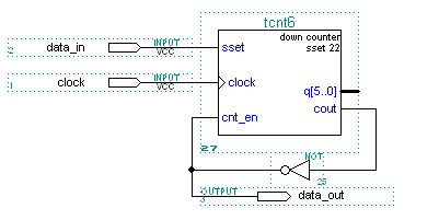
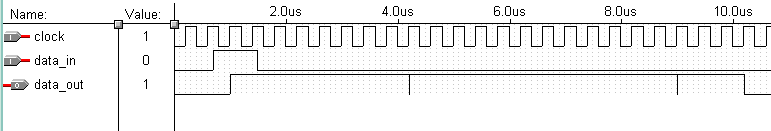
Making a short pulse longer
It sometimes can happen that a pulse is too short, so it has to be made longer
There may be exteme cases, where a signal of an FPGA running at 100MHz or so
has to be connected to a slow microcontroller. Then the extension of the pulse
with one or a few more flipflops is not appropriate. A counter is the preferred
solution, as it only uses log2(n) flipflops compared to the linear solution.
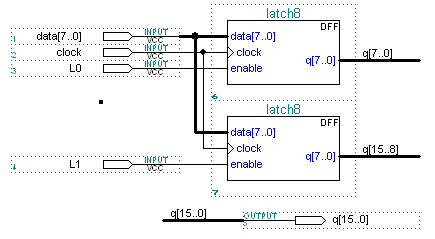
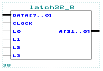
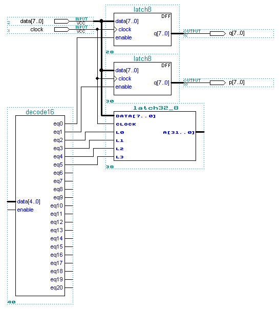
Using parallel registers to interface to the external world
Parallel registers are a great way to interface to some microcontroller.
The microcontroller can set some FPGA internal values as 8bit (or whatever) chunks
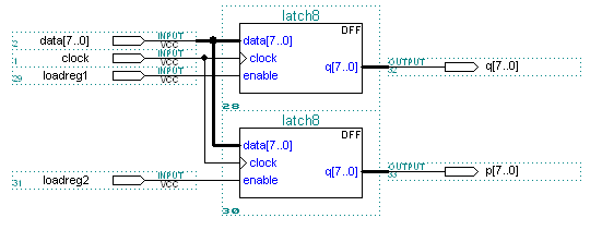
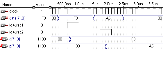
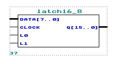
Should 16 bit be loaded as two times 8bit, MaxPlus2 in this case allows to
build a combined element, with own file, own name and own icon.
likewise is a 32bit register or whatever size built.
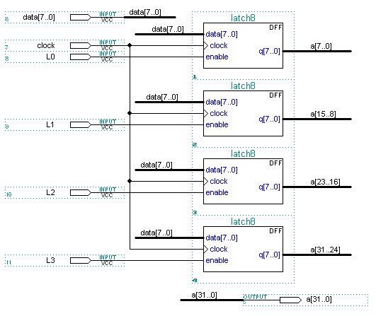
From a certain number of registers up, having a load-control line for each
becomes uneconomic. Then a decoder is the choice.
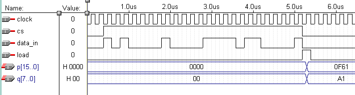
Using serial registers to interface to the external world
Serial registers are a great way to interface to some microcontroller.
The microcontroller can set some FPGA internal values as 8bit (or whatever) chunks
At the expense of reduced speed, some pins may be saved by shifting the data
serially. Shown here is a 16bit register implementation.
Required are just 4 pins: Clock, CS, Data and Load.
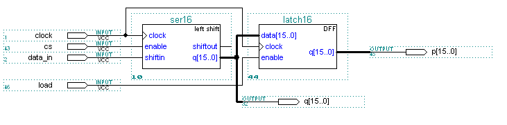
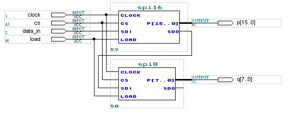
This unit appears later as SPI16 with an own icon
At the expense of a accordingly more clockcycles, multiple serial registers
can be chained, without spending more of the precious pins.
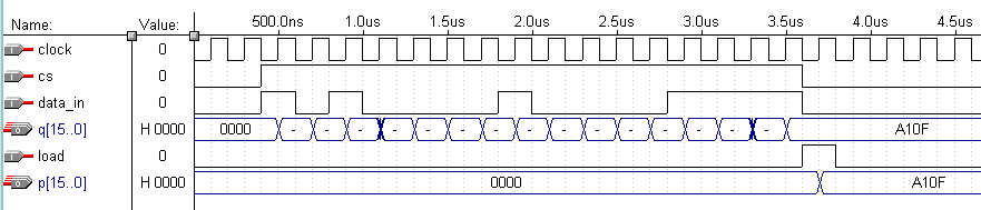
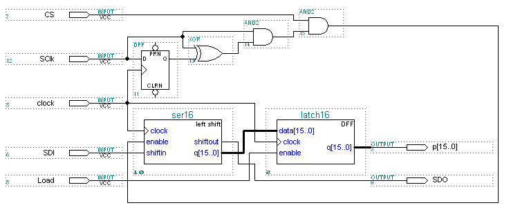
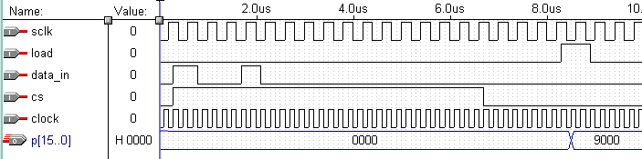
Using serial register with a slower clock
When the FPGA and the microcontroller are not running at the same clock
speed, an additional signal, the SClk has to be added. Data is assumed
valid on its rising edge. Upon this rising edge, an enable is formed and used
as clock enable in the previous example.
disclaimer
Code shown here is taken from recent projects. It may appear to have strange
features, as the context is missing. The code may or may not be tested, as
in the process of reediting for this publishing, names may have been incorrectly
changed, and lines may be missing. The code may serve as reference to pass the
idea only. It may not be optimal, and may have bugs. There is no right to get it
fixed and no liability whatsoever. Send me a mail
if you find a bug though.
electronics home
ibrt home
last updated : 08.nov.03 or perhaps later
Copyright (99,2003) Ing.Büro R.Tschaggelar